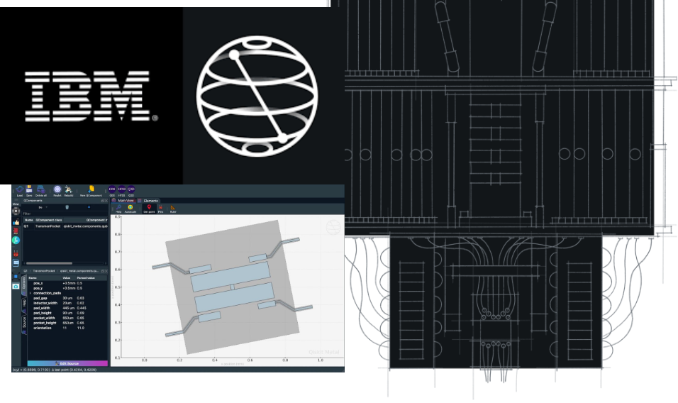
Qiskit Metal: Superconducting Chip Design
Why Qiskit Metal?
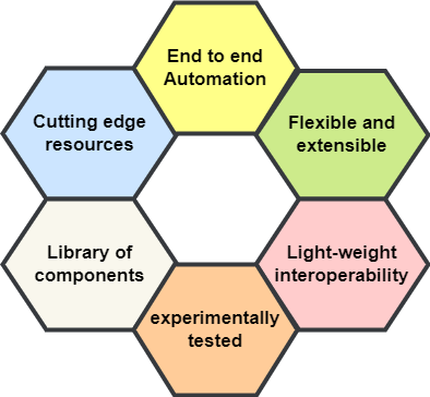
1-End to end Automation: In metal we can choose from a list of available tools or connect our own through a flexible plug-in interface that allows us to orchestrate device design from within Metal.
2-Flexible interface: GUI view, Jupyter notebook view, Simulator view,etc..
Extensible: User-friendly Python API and library of tools allow you to define your own custom quantum components.
3-Light weight interoprability : It is an All-in-one platform powerful programming paradigm to unify design, simulation, and quantum analysis.
4- Experimentally Tested : Metal utilizes quantization methods and techniques from both the community and our own development.
5-Library of components: We can take benefit from built-in and community-developed library of quantum device components.
6-Cutting edge Resources: Built-in best practices and the latest simulation and analysis techniques helps us to test and build a shared set of cutting edge resources.
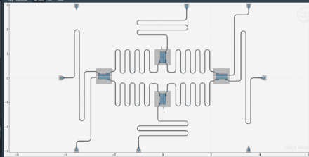
let's try it out by designing a 4 qubit chip design.
Target Chip Design:

Step 1 :
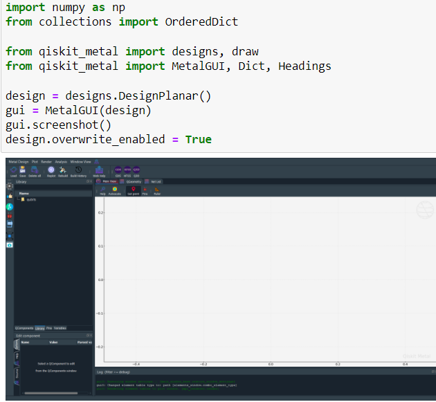
- from collections import OrderedDict : This will import the OrderedDict class from the collections module.It will help to remember the order of the keys that were inserted into it,they will be returned in the order they were added.
- from qiskit_metal import designs, draw : This will import the designs and draw modules from the qiskit_metal library. The designs module contains functions for creating and manipulating different types of quantum circuit designs, while the draw module provides functions for visualizing and drawing the designs.
- from qiskit_metal import MetalGUI, Dict, Headings : This will import the MetalGUI , Dict and Headings classes from the qiskit_metal library. The MetalGUI class is the main class for creating and interacting with a graphical user interface (GUI) for designing and simulating quantum circuits. The Dict and Headings classes are used for formatting and displaying the data in the GUI.
- design = designs.DesignPlanar() : This will creates a new instance of the DesignPlanar class from the designs module. This class is used for creating and manipulating planar quantum circuits.
- gui = MetalGUI(design) : Ths will create a new instance of the MetalGUI class and initializes it with the design object created in the previous step. This creates a new GUI window with the given design and makes it ready for interaction.
Step2:
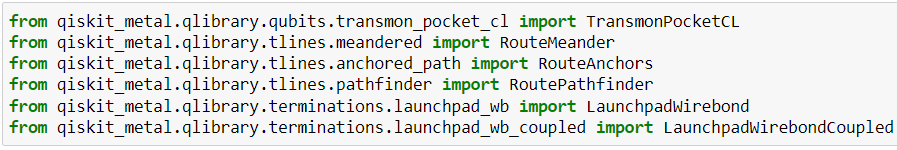
- from qiskit_metal.qlibrary.qubits.transmon_pocket_cl import TransmonPocketCL
Note: This will be used for creating and working with transmon qubits, which are a type of superconducting qubit.
2. from qiskit_metal.qlibrary.tlines.meandered import RouteMeander
Note:This will be used for creating and working with meandered transmission lines, which are a type of transmission line used in superconducting quantum circuits.
3. from qiskit_metal.qlibrary.tlines.anchored_path import RouteAnchors
Note:This will be used used for creating and working with anchored transmission lines, which are a type of transmission line used in superconducting quantum circuits.
4. from qiskit_metal.qlibrary.tlines.pathfinder import RoutePathfinder
Note: This will be used for finding an optimal path for routing the transmission lines in a superconducting quantum circuit.
5. from qiskit_metal.qlibrary.terminations.launchpad_wb import LaunchpadWirebond
Note:This will be used for creating and working with launchpad wirebond terminations, which are a type of termination used in superconducting quantum circuits.
6. from qiskit_metal.qlibrary.terminations.launchpad_wb_coupled import LaunchpadWirebondCoupled
Note: This is similar to the LaunchpadWirebond class, but it is used for creating and working with launchpad wirebond terminations that are coupled to other transmission lines.
Step3:
These lines of code are modifying the properties of the design object.
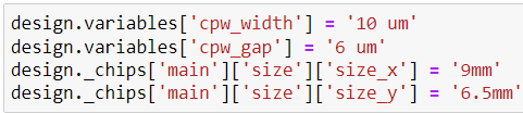
1. design.variables['cpw_width'] = '10 um' : This will set the value of the cpw_width variable in the design object to "10 um".
Note: This variable represents the width of a coplanar waveguide (CPW) transmission line, which is a type of transmission line used in superconducting quantum circuits. The units of the value are given in micrometers (um)
2. design.variables['cpw_gap'] = '6 um' : This will set the value of the cpw_gap variable in the design object to "6 um".
Note: This variable represents the gap between the center conductor and ground planes of a CPW transmission line. The units of the value are given in micrometers (um).
3. design._chips['main']['size']['size_x'] = '9mm' : This will set the value of the size_x variable in the size dictionary of the main chip in the design object to "9mm".
Note:This variable represents the size of the chip along the x-axis. The unit is in millimeters (mm).
4. design._chips['main']['size']['size_y'] = '6.5mm' : This will set the value of the size_y variable in the size dictionary of the main chip in the design object to "6.5mm".
Note:This variable represents the size of the chip along the y-axis. The unit is in millimeters (mm).
These values are used to define the physical properties of the planar quantum circuit in the design, such as the width, gap, size and other properties of the transmission lines and chips.
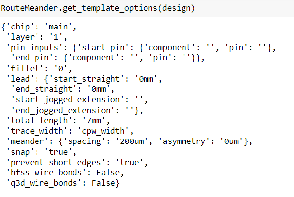
Step4:
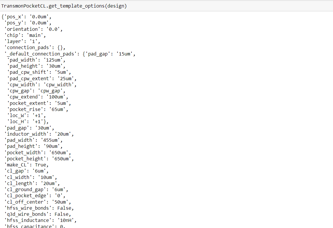
Note: This method is used to get the available options for creating a transmon qubit based on the design object passed as an argument.
Step5:
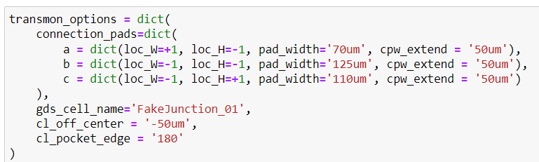
This code creates a dictionary object transmon_options which stores a set of options for creating a transmon qubit in a superconducting quantum circuit. These options include:
- connection_pads : a dictionary containing 3 different key-value pairs, where each key represents a connection pad, and the value is representing the properties of the connection pad such as loc_W ,loc_H ,pad_width and cpw_extend . loc_W and loc_H represents the location of the pad on the chip, pad_width is the width of the pad, and cpw_extend is the distance between the pad and the end of the transmission line connected to it.
- gds_cell_name : It is a name of the GDS layout file that will be used to create the transmon qubit.
- cl_off_center : It is distance between the center of the qubit and the center of the coupling loop.
- cl_pocket_edge : It is a distance between the edge of the qubit and the edge of the coupling loop pocket.
Step6:
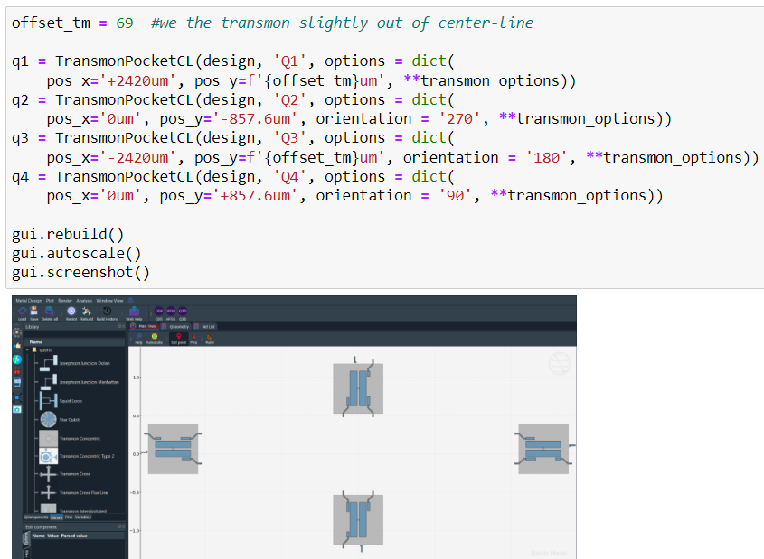
- offset_tm = 69 : It is a variable that holds an offset value of 69 micrometers (um) which will be used to slightly move the transmon qubits out of the center-line.
- q1 = TransmonPocketCL(design, 'Q1', options = dict(pos_x='+2420um',pos_y=f'{offset_tm}um', **transmon_options)) : This will create a new transmon qubit named 'Q1' and adds it to the design object. The pos_x and pos_y options specify the position of the qubit on the chip in micrometers. The **transmon_options is used to pass the options defined in the transmon_options dictionary to the TransmonPocketCL class.
Likewise , we will create qubits q2,q3,q4.
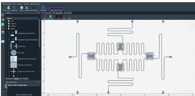
After the qubits are added, gui.rebuild() and gui.autoscale() methods are called to rebuild and autoscale the GUI window, which will update the display of the design with the new qubits.
Step7:
Note: It's important to note that this method is only used to get the options for creating a meandered transmission line based on the design object, it does not actually create the transmission line.
Step8:
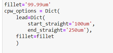
This code creates a dictionary object called cpw_options which stores a set of options for creating transmission line in a superconducting quantum circuit. These options include:
- lead : a dictionary containing two key-value pairs, start_straight and end_straight representing the length of the straight section at the start and end of the transmission line. The value of both are given in micrometers (um).
- fillet : a string variable representing the radius of the rounded corners of the transmission line. The value is given in micrometers (um).
Step9:
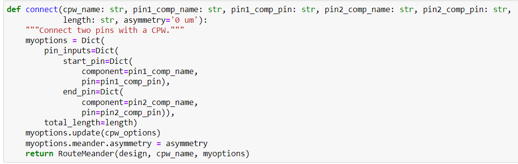
This code defines a function called connect() that is used to connect two pins of two different components with a transmission lines.
The function takes in several parameters:
- cpw_name : a string representing the name of the transmission line
- pin1_comp_name : a string representing the name of the first component
- pin1_comp_pin : a string representing the name of the pin on the first component
- pin2_comp_name : a string representing the name of the second component
- pin2_comp_pin : a string representing the name of the pin on the second component
- length : a string representing the total length of the transmission line
- asymmetry : a string representing the asymmetry of the meander layout
The function uses the Dict class from the qiskit_metal library to create a dictionary object called myoptions .This dictionary contains options for creating the CPW transmission line such as the pin_inputs which is a dictionary containing two key-value pairs- start_pin and end_pin , which is representing the first and second component and the pin of the component that the CPW will connect.
The total_length option is set to the value of the length parameter passed to the function.
Note :The cpw_options created earlier is then updated by calling myoptions.update(cpw_options)
Finally, the function creates an instance of the RouteMeander class, passing it the design object, cpw_name and myoptions .This creates the CPW transmission line, connects the two pins, and adds it to the design. The function then returns the created instance of the RouteMeander class.
Step10:
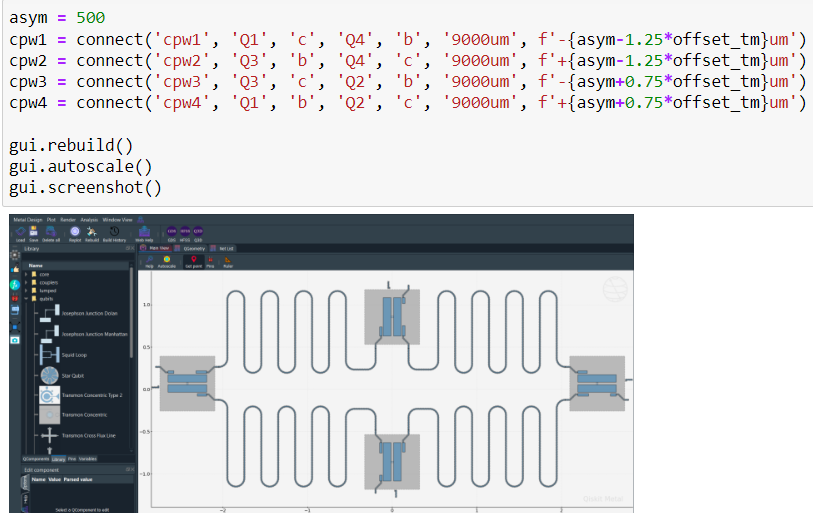
These lines of code create four CPW transmission lines, cpw1 , cpw2, cpw3 and cpw4 using the connect() function defined earlier and add them to the design object.
- asym = 500 is a variable that holds an asymmetry value of 500 micrometers (um) which will be used to create the asymmetry of the meander layout of the CPW transmission line.
- cpw1 = connect('cpw1', 'Q1', 'c', 'Q4', 'b', '9000um', f'-{asym-1.25*offset_tm}um') : This will create a new CPW transmission line named 'cpw1' and connects the 'c' pin of the 'Q1' component to the 'b' pin of the 'Q4' component. The total length of the CPW is 9000um and the asymmetry of the meander layout is calculated by subtracting 1.25 times the offset_tm from the asym variable.
- cpw2 = connect('cpw2', 'Q3', 'b', 'Q4', 'c', '9000um', f'+{asym-1.25*offset_tm}um') : This will create a new CPW transmission line named 'cpw2' and connects the 'b' pin of the 'Q3' component to the 'c' pin of the 'Q4' component. The total length of the CPW is 9000um and the asymmetry of the meander layout is calculated by adding 1.25 times the offset_tm to the asym variable.
- cpw3 = connect('cpw3', 'Q3', 'c', 'Q2', 'b', '9000um', f'-{asym+0.75*offset_tm}um'): This will create a new CPW transmission line named 'cpw3' and connects the 'c' pin of the 'Q3' component to the 'b' pin of the 'Q2' component. The total length of the CPW is 9000um and the asymmetry of the meander layout is calculated by subtracting 0.75 times the offset_tm from the asym variable.
- cpw4 = connect('cpw4', 'Q1', 'b', 'Q2', 'c', '9000um', f'+{asym+0.75*offset_tm}um'): This will create a new CPW transmission line named 'cpw4' and connects the 'b' pin of the 'Q1' component to the 'c' pin of the 'Q2' component. The total length of the CPW is 9000um and the asymmetry of the meander layout is calculated by adding 1.25 times the offset_tm to the asym variable.
Step11:
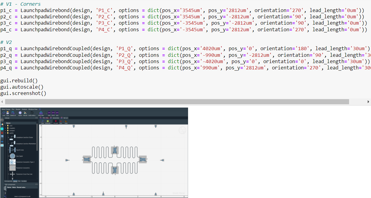
These lines of code create several launchpad wirebond terminations and add them to the design object.
Route- V1 launchpads - Chargelines to corners.
- p1_c = LaunchpadWirebond(design, 'P1_C', options = dict(pos_x='3545um', pos_y='2812um', orientation='270', lead_length='0um')): This will create a launchpad wirebond termination named 'P1_C' with the given options, specifying the position, orientation, and lead length of the termination.
- p2_c = LaunchpadWirebond(design, 'P2_C', options = dict(pos_x='3545um', pos_y='-2812um', orientation='90', lead_length='0um')): This will create a launchpad wirebond termination named 'P2_C' with the given options, specifying the position, orientation, and lead length of the termination.
- p3_c = LaunchpadWirebond(design, 'P3_C', options = dict(pos_x='-3545um', pos_y='-2812um', orientation='90', lead_length='0um')):This will create a launchpad wirebond termination named 'P3_C' with the given options, specifying the position, orientation, and lead length of the termination.
- p4_c = LaunchpadWirebond(design, 'P4_C', options = dict(pos_x='-3545um', pos_y='2812um', orientation='270', lead_length='0um')): This will create a launchpad wirebond termination named 'P4_C' with the given options, specifying the position, orientation, and lead length of the termination.
Route-V2 launchpads - Exchange Coupler Lines to Edges.
- `p1_q = LaunchpadWirebondCoupled(design, 'P1_Q', options = dict(pos_x='4020um', pos_y='0', orientation='180', lead_length='30um')): This will create a launchpad wirebond termination named 'P1_Q' of coupled type with the given options, specifying the position, orientation, and lead length of the termination.
- p2_q = LaunchpadWirebondCoupled(design, 'P2_Q', options = dict(pos_x='-990um', pos_y='-2812um', orientation='90', lead_length='30um')):This will create a launchpad wirebond termination named 'P2_Q' of coupled type with the given options, specifying the position, orientation, and lead length of the termination.
- p3_q = LaunchpadWirebondCoupled(design, 'P3_Q', options = dict(pos_x='-4020um', pos_y='0', orientation='0', lead_length='30um')): This will create a launchpad wirebond termination named 'P3_Q' of coupled type with the given options, specifying the position, orientation, and lead length of the termination.
- p4_q = LaunchpadWirebondCoupled(design, 'P4_Q', options = dict(pos_x='990um', pos_y='2812um', orientation='270', lead_length='30um')) : This will create a launchpad wirebond termination named 'P4_Q' of coupled type with the given options, specifying the position, orientation, and lead length of the termination.
Step12:
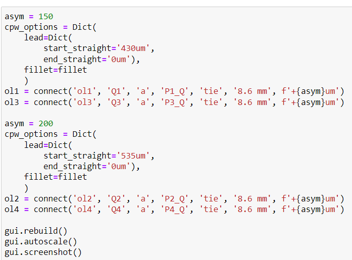
These lines of code create four additional CPW transmission lines (ol1, ol2, ol3, and ol4) and connect them to the launchpad wirebond terminations.
- cpw_options = Dict(lead=Dict(start_straight='430um', end_straight='0um'), fillet=fillet) will set the lead and fillet options for the CPW transmission lines.
- ol1 = connect('ol1', 'Q1', 'a', 'P1_Q', 'tie', '8.6 mm', f'+{asym}um') : This will create a new CPW transmission line named 'ol1' and connects the 'a' pin of the 'Q1' component to the 'tie' pin of the 'P1_Q' component.
- ol3 = connect('ol3', 'Q3', 'a', 'P3_Q', 'tie', '8.6 mm', f'+{asym}um'): This will create a new CPW transmission line named 'ol3' and connects the 'a' pin of the 'Q3' component to the 'tie' pin of the 'P3_Q' component.
- ol2 = connect('ol2', 'Q2', 'a', 'P2_Q', 'tie', '8.6 mm', f'+{asym}um'): This will create a new CPW transmission line named 'ol2' and connects the 'a' pin of the 'Q2' component to the 'tie' pin of the 'P2_Q' component.
- ol4 = connect('ol4', 'Q4', 'a', 'P4_Q', 'tie', '8.6 mm', f'+{asym}um') :This will create a new CPW transmission line named 'ol4' and connects the 'a' pin of the 'Q4' component to the 'tie' pin of the 'P4_Q' component.
The total length of the CPW is 8.6mm.
Step13:
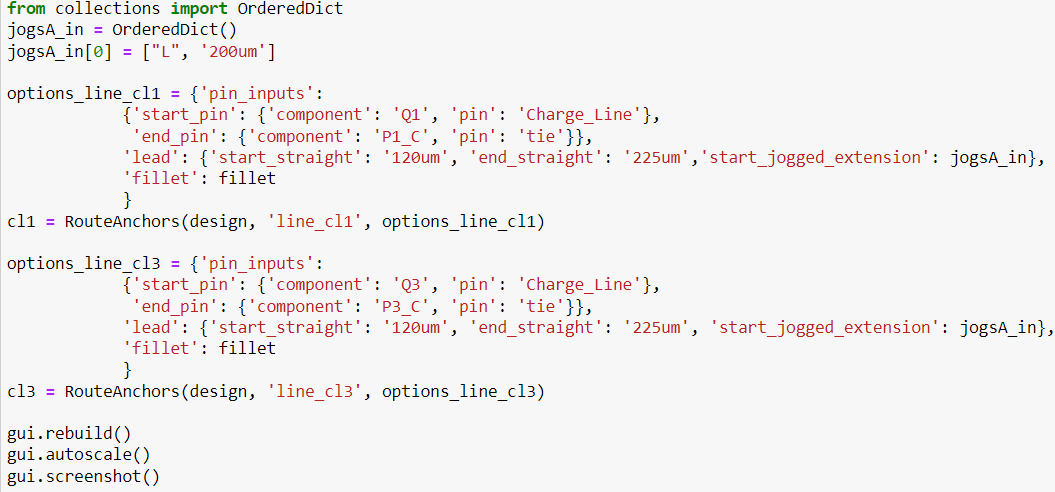
These lines of code create two charge lines, cl1 and cl3 and add them to the design object.
- jogsA_in = OrderedDict() : This will create an empty ordered dictionary named jogsA_in.
- jogsA_in[0] = ["L", '200um'] : This will add an entry to the ordered dictionary, where the key is 0 and the value is a list containing the letter "L" .
- options_line_cl1 and options_line_cl3 : This will create a variable options_line_cl1 and options_line_cl3 that holds the options for the cl1 and cl3 charge line, which includes the start and end pins of the line, the lead options such as start_straight, end_straight, and start_jogged_extension and the fillet options.
- cl1 , cl3 : This will create a new charge line named cl1 and cl3 using the RouteAnchors class , it is then added to the design object using the options specified in the options_line_cl1 and options_line_cl3 variable.
Step14:
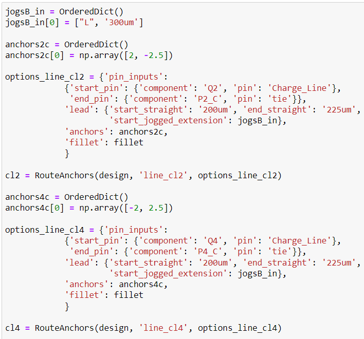
These lines of code create two additional charge lines, cl2 and cl4 , and add them to the design object.
- jogsB_in = OrderedDict() creates an empty ordered dictionary named jogsB_in.
- `jogsB_in[0] = ["L", '300um'] This will add an entry to the ordered dictionary, where the key is 0 and the value is a list containing the letter "L".
- anchors2c and anchors4c = OrderedDict() creates an empty ordered dictionary.
- anchors2c[0] and anchors4c[0] = np.array([2, -2.5]) adds an entry to the ordered dictionary, where the key is 0 and the value is a numpy array containing the x and y coordinates of the anchor
- options_line_cl2 and options_line_cl4 : This will create a variable options_line_cl2 and options_line_cl4 that holds the options for the cl2 and cl4 charge line, which includes the start and end pins of the line, the lead options such as start_straight, end_straight, and start_jogged_extension, anchor options and the fillet options.
- cl2 and cl4: This will create a new charge line named cl2 and cl4.
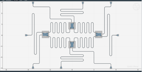
- gui.rebuild() regenerate the graphical representation of the design object.
- gui.autoscale() adjusts the view of the graphical representation so that all the elements of the design fit in the window.
Here,we have obtained a design of our targeted superconduting 4 qubits chip.